Samsung is continuing to push forward its plans to become the largest semiconductor contract foundry by showcasing its latest tech to prospective partners in order to lure them away from TSMC. Samsung might well be one of the biggest tech companies in the world, but it wants to grab a bigger slice of the contract manufacturing pie TSMC has been gobbling down recently. At the moment the Taiwanese pureplay foundry has around 50% of the contract manufacturing market while Samsung is trailing behind at just under 15%.
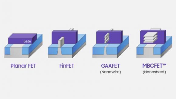
In order to steal a march on TSMC, the Korean giant has given out the process design kit for its advanced 3nm Gate-All-Around Field Effect Transistor (GAAFET) process in order for potential customers to get an early start on the tough design work needed to create chips on the brand new, super-advanced node.
The bafflingly miniscule 3nm process is the first of Samsung’s nodes to move beyond the existing FinFET transistor design and onto the GAA layout. Gate-All-Around transistors provide greater control over the flow of electricity than FinFET, particularly at this smaller scale.
The Yonhap News Agency reported on the recent Samsung Foundry Forum, held in Santa Clara, where it invited 800 semiconductor bods and customers to see its new process technology advancements. It says Samsung is “actively promoting” its new process technology in order to catch up with TSMC and cut into its lucrative 50% market share.
Top chips: These are the best CPUs for gaming right now
The 3nm GAA process isn’t the only one the company has been shopping around either, there are another four FinFET process nodes available before we get down into that freakishly small lithography, all of which sport the new extreme ultraviolet (EUV) tech. Samsung has the 7nm, 6nm, 5nm, and 4nm nodes all still to come, though we’re not entirely sure whether those are all derivatives of the same essential process.
TSMC has 7nm+ and 6nm nodes as derivatives of the same 7nm process that AMD is using for both its Ryzen 3000 processors and the upcoming Radeon Navi graphics cards. That means the subsequent designs will all be more or less compatible with each other, significantly cutting down the time to manufacture moving to the more advanced nodes.
TSMC’s 5nm process, however, is a whole new design, requiring a fresh approach to the makeup of chips based on that lithography, potentially making it more expensive, and take longer for companies to get their silicon ready for the new node.
When will 5nm silicon appear?
Samsung, however, seems to be retaining compatibility for all of its four FinFET nodes, potentially meaning it could get product out of its fabs at 4nm while TSMC is still squeezing 5nm out of the factory doors. Both companies are aiming for mass production of their respective 5nm nodes in the first half of 2020, but it may be faster for Samsung’s customers to transition down to 4nm. That could give Samsung a bit of a process lead, and might swing market share in its favour.
And that could be the reason TSMC’s board has recently approved nearly $4bn of extra capital for its advanced-node manufacturing. The money has been earmarked for the purpose of expanding and upgrading TSMC’s capacity for advanced nodes, and for continued research and development.
With a company the size of Samsung breathing down its neck I wouldn’t be surprised if TSMC was starting to feel the heat and is responding to the imminent silicon onslaught.


