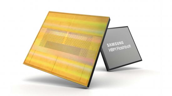
Next-gen GPUs have the potential for a vast amount of high-performance memory being strapped onto the silicon thanks to the new Samsung HBM2E stacks which have just been launched into the market. The new HBM2E standard has been specified by the JEDEC group and both Samsung and SK Hynix have been developing new speedy chip stacks for the next generation of graphics cards.
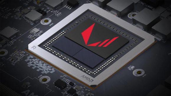
Though realistically you’re unlikely to see the fruits of their labour in your next GPU purchase unless you’re Betsy Big Pockets with a wallet to match. The high bandwidth memory (HBM) dream was briefly flirted with in desktop graphics cards, with the AMD Vega graphics cards – the RX Vega 64, RX Vega 56, and Radeon VII – but since then we’ve not seen hide nor silicon hair of it outside of the datacentre.
Sure, you could’ve bagged yourself an Nvidia Titan V and jammed that into your gaming rig for a Volta/HBM2 combo, but you’d have needed to drop $3,000 on the card alone. The new HBM2E spec, however, makes even that GPU’s 12GB of high bandwidth memory look lightweight.
Samsung is starting to ship 16GB stacks of its new Flashbolt HBM2E (via Guru3D), strap a couple of those onto your new GPU and you’re looking at a graphics card with 32GB of memory that’s capable of a stable 3.2Gbps transfer rate. And that’s going to give you a total bandwidth of 410GB/s per stack.
Samsung does say that its mew memory is also capable of getting up to 4.2Gbps per stack, which would deliver up to 538GB/s in the future. And in that future Samsung will be working to the full JEDEC HBM2E spec that allows up to 12 dies to be stacked on top of each other.
At the moment Samsung’s Flashbolt chips have eight layers of 16Gb HBM2E dies, for a total of 16GB of total memory per stack. With 12 layers you’re looking at a maximum of 24GB per stack. A datacentre GPU of the future could easily come rocking 96GB of super-fast memory thanks to the new standard.
It’s not just Samsung getting in on the HBM2E dance as SK Hynix too will be shipping its own HBM2E stacks this year too. It claimed to have a 3.6Gbps stable transfer rate, and it will be interesting to see if that stays the same when the SK Hynix chips are fully available.
But where are we going to see the new HBM2E stacks used? Well, Nvidia is expected to start talking up its next-gen GPU architecture at the GTC event in March, and that will likely feature datacentre silicon first. Especially as the new Cray Big Red 200 machine is going to be doing all the AI-ing at Indiana University with the next-gen Nvidia GPUs later on this year…

