By 2021 Samsung expects to be a year ahead of foundry rivals TSMC, in terms of advanced process production, and two or three years ahead of technology rivals, Intel. When the Korean tech giant starts mass producing its 3nm gate-all-around lithography in two years time the competition will potentially be scrabbling around to catch up, with Samsung potentially mopping up the big chip-making contracts with its new design.
Right now TSMC is cleaning up in terms of high-performance PC chip manufacturing, with AMD adopting its 7nm process wholesale for both its upcoming Ryzen 3000 processors, as well as the incoming AMD Navi graphics cards. It has also committed to the 7nm+ process for the Zen 3 CPUs too. Nvidia is also expected to use TSMC for its next-gen graphics technology, though has reportedly already started working with Samsung on advanced nodes.
But if Samsung can indeed push its technology to the point where it has a process lead over TSMC by as much as twelve months, then a lot more of that contract work could start filtering over from Taiwan to Korea.
And that’s exactly how Samsung wants to play it, expanding its foundry presence to put pressure on TSMC as the current number one player with 50% market share. The fact Samsung is expected to cede semiconductor market lead to Intel once more in 2019, driven by the dip in demand DRAM and NAND flash manufacturing, must also add some extra needle to this push for foundry dominance.
Top chips: These are the best CPUs around today
At the Samsung Foundry Forum, where it announced the company had already given out the process design kit for its 3nm gate-all-around (GAA) technology to prospective clients, Samsung has been impressing industry insiders with its progress against the stiff competition it faces in the market.
“Samsung is ahead of TSMC in GAA by probably 12 months,” says Handel Jones of consultants International Business Strategies. “Intel is probably two to three years behind Samsung.”
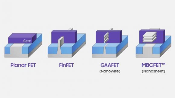
This is because, while the likes of Intel and TSMC are working on GAA transistors themselves, Samsung has been working on a proprietary version it’s calling multi-bridge channel field effect transistors (or MBCFET if you’re into a little brevity). Instead of the nanowire construct of other companies’ GAAFET designs Samsung uses nanosheets which decreases the process complexity and allows for a larger current per stack to be used. It also has better utilisation of die area, and potentially allows for more stacked nanosheets per transistor to improve performance.

The MBCFET design is also compatible with Samsung’s existing process tools and production methodology. The same kit it uses to manufacture current-gen FinFET designs should be usable for its take on GAA transistors, which will shorten time to market and the cost efficiency of the process.
In terms of just a straight FinFET vs MBCFET argument, Samsung is promising 50% lower power consumption, 30% higher performance, and a reduction in area of around 45%, all compared to a 7nm FinFET design.

The process is going to hit volume production in 2021, likely with lower-performance mobile processor, with high-end GPUs and CPUs expected to follow in 2022. If AMD continues to follow its current cadence that could present the potential for a switch from TSMC to a 3nm MBCFET Samsung design for Zen 5. Though that might be expecting a little much…
But from there Samsung is already looking towards 2nm manufacturing, based upon the MBCFET technology, with visibility to 1nm and beyond. After that we’re going to have to start coming up with a new measurement standard.

