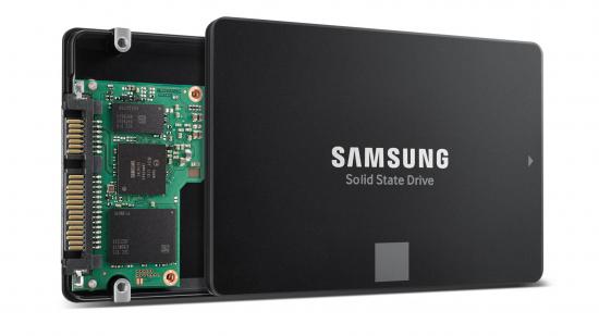
The race to mass manufactured 100+ layer NAND Flash heats up as Samsung announces its sixth generation V-NAND in 256Gb, 3-bit (TLC) chips. This marks the industry’s first attempt to incorporate over 100 layers across a single stack. Aided by a “speed-optimised circuit design,” Samsung plans on stacking multiple 100+ layer chips within high-density SSDs up to 300 layers deep.
The company claims to have secured the “industry’s highest performance, power efficiency, and manufacturing productivity” with the latest 3D memory tech, which utilises channel hole etching to increase cell density by 40% over 96-layer fifth generation V-NAND. This is achieved by layering 136 layers of an electrically conducive mold stack, and then piercing holes all the way through with a tiny, fancy holepunch to create uniform charge trap flash (CTF) cells.
However, as the cell height increases, error and read latencies also increase. To address this issue as layers increase, Samsung will roll out a new speedy circuit design. This will help achieve faster transfer speeds of below 450μs write and 45μs read. That’s a 10% bump to fifth gen V-NAND and a 15% decrease in power demand.
It is also planning to roll-out 300-layer SSDs with multiple 100-layer stacks, made possible without performance degradation thanks to the new circuit design.
“Thanks to this speed-optimized design,” it says in a press release, “Samsung will be able to offer next-generation V-NAND solutions with over 300 layers simply by mounting three of the current stacks, without compromising chip performance or reliability.”
Vertically stacked NAND is utilised to increase density without affecting reliability, which had been a limitation with planar, or single level, NAND.
The first SSD built upon Samsung’s new tech will be a 256GB SSD shipping to OEMs and built on the limited speed SATA interface, precursor to a complete mass manufacturing roll-out of sixth generation products built upon 512Gb chips in the second half of the year.
Samsung isn’t the first to over 100 layers of NAND flash, however, and its latest achievement comes just a little after SK Hynix announced its own 128-layer 4D (marketing) TLC NAND utilising PUC, or Peri. Under Cell, technology. This is also set to start shipping in the second half of 2019.
Want to discuss this article? Head over to Facebook or Twitter.
