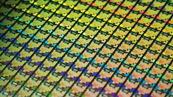
TSMC is looking to take its 7nm EUV process node on the road in March. The company’s current 7nm process recently made its gaming debut with the Radeon VII, the “world’s first 7nm gaming GPU” from AMD, showing off what a difference a process node can make. But to keep Moore’s momentum up, the fab has now announced an EUV-augmented 7nm process will be ready to roll out in March.
The pure-play fab – it doesn’t make any of its own chips – currently takes care of most of Nvidia’s product stack, including Nvidia Turing graphics cards. However, it also recently picked up most of AMD’s business once GlobalFoundries, ex-AMD subsidiary and once-favoured foundry, said no more (no Moore?) to investing further in 7nm R&D.
There’s now speculation growing that Global Foundries is seeking a buyer. The company has been rapidly downsizing: selling off fabs, cutting staff, and amending agreements with AMD and the Chengdu municipality in China. Efforts to streamline the company have led onlookers to believe the company’s owners, Abu Dhabi’s Advanced Technology Investment, may be looking to sell.
But while one fab fumbles, another is ready to pick up the slack as the foundry club grows ever-more exclusive. TSMC is now reportedly (via DigiTimes) picking up 18 EUV-capable systems from ASML, the lithographic equipment manufacturers.
Silicon connoisseur: These are the best graphics cards
EUV, or extreme ultraviolet, will reduce the complexity required to produce such dense process nodes as 7nm – and later this year, 5nm. It works by utilising a wavelength of only 13.5nm, meaning fabs can reduce the optical trickery required to shrink chip designs down.
TSMC had begun risk production of 7nm EUV last year, but this March the fab plans on pushing its cutting-edge node to the wider market. Samsung also began volume production using 7nm EUV last year and Intel’s recent fab expansion flurry has been tied to EUV expansion.
TSMC’s current 7nm process node has proven to be quite capable in its own right without even all that EUV technology abuzz. AMD’s 3rd Gen Ryzen teaser proved the red team’s latest 7nm chiplet silicon was capable of beating Intel’s finest with far less juice, and AMD’s Radeon VII – essentially a rehashed Vega – easily surpasses the old 14nm Vega 64 GPU thanks to the denser node and a couple extra HBM2 dies.
We know AMD intends to utilise the 7nm+ process node for its next-generation GPU architecture following AMD Navi in 2020, and for it’s Zen 3 CPU update too. And while Nvidia hasn’t confirmed a timeframe for its 7nm efforts, the way things are shaping up it looks like it too will be on the EUV train once its next-generation GPUs arrive.
