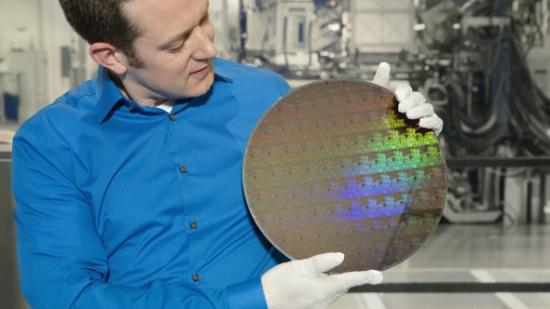
IBM have created the first manufacturing process capable of delivering 5nm chips, a silicon marvel that packs in 30 billion transistors and performs 40% better than commercial 10nm chips. That’ll be why the fella in their promotional image holding the wafer looks so in love, then.
The future of gaming rigs is creeping ever closer, but in the meantime check out our guide to the best gaming CPUs to make sure you have the best tech of today.
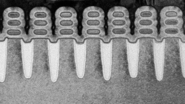
That’s right people – companies other than Intel are making waves in silicon manufacturing. IBM teamed up with Samsung and GlobalFoundries to put together their 5nm demonstration which makes use of horizontal gate-all-around (GAA) transistors and extreme ultraviolet (EUV) lithography to achieve their tiny size.
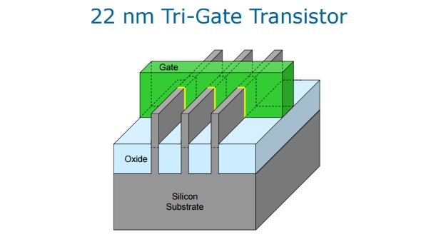
The current FinFET (or Tri-Gate if you’re Intel) transistor design was an advance over the flat, planar transistors, and uses solid, extruded 3D ‘fins’ from the silicon base allowing for a larger conducting channel through the off-on gate. GAAFETs, however, increase the size of the conducting channel even further by wrapping the silicon nanosheets on all four sides, with multiple sheets stacked on top of each other. This increased conducting channel means they can squeeze more juice through in the same space, allowing for the huge increase in transistor density IBM are touting.

The 30 billion transistors IBM can fit on the chip (which is the size of a fingernail) is a full 10 billion more than a 7nm FinFET chip of a similar size. Using EUV means IBM manufacturers can adjust the width of the chip’s silicon nanosheets, allowing them to fine-tune performance.
For reference there are only 12 billion transistors in Nvidia’s current 16nm GPUs.

GAAFET chips may be able to become as small as 3nm in the future due to the design of their transistors. Even now, though, the 5nm process they’re showing off can theoretically deliver a 40% performance improvement over a 10nm chip running on the same power, or 75% less power consumption when performing at the same level. In other words, either your games or your electricity bill will thank you. Less power consumption would also mean that laptop gamers are rushing to their nearest wall socket less often.
We don’t know what 10nm chip they’re referring to, however. They’re unlikely to have been testing Intel’s unreleased 10nm lithography so we assume the performance benefits are measured against Samsung’s own 10nm node.
Chips created using a process like this could potentially result in a pretty big performance hike in CPUs, then. The only trouble is that high-performance PC components pump out loads of heat and therefore require bulky (and sometimes very expensive) cooling methods. A 5nm chip built like this will draw less power than its contemporaries, but it’s not exactly going to make PC cooling obsolete.

However, research published in January of this year shows other materials may take up silicon’s mantle in CPUs, making cooling as we know it a thing of the past. The study showed that the law-defying metal vanadium oxide is capable of conducting electricity without conducting heat, a discovery that could entirely change how PC components are built, and mean we could run chips at speeds that previously would’ve kicked out the heat of the sun.
It’s still early days for this tech, however, so it’s best not to expect a 5nm chip in your PC any time soon. We’ll be pretty close to that scale in less than three years, though, as AMD have already committed to hitting 7nm with their second-generation Zen CPUs well before 2020.
Thanks Ars Technica.
