AMD’s chief tech officer, the Papermaster, has announced the their plans to transition directly from the current 14nm LPP production process down to the new 12nm LP lithography in 2018.
Don’t want to wait for a new processor? Check out our pick of the best CPUs for gaming.
Everyone has a Tech Conference these days. I’ve got one I run out of the back of my garage where I’ve recently discussed such important topics as the new production process I’m thinking of using in my next-gen apple crumble and the age old spade vs. shovel debate. Attendance was well down this year, though… damn Brexit. I guess as one of the few leading edge silicon manufacturers out there, however, Global Foundries has more call to run one and, arguably, is more newsworthy.
It was at this year’s Global Foundries Technology Conference that Mark Papermaster announced next year’s transition down to the smaller node, with Global Foundries themselves following this up by stating that actual 12nm LP production would begin right at the start of 2018. That means we shouldn’t have too long to wait for new, hopefully more efficient, AMD silicon.

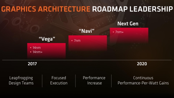
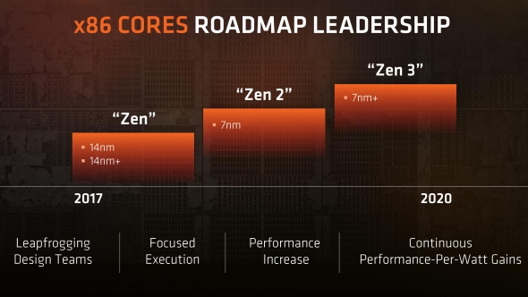
This looks like it will be the lithography which forms the basis of the touted AMD Vega and AMD Ryzen refreshes. Previous roadmaps released by them have shown the two current-gen GPU and CPU technologies are set for some tweaks before we see any movement on the upcoming Navi and Zen 2 architectures, both of which are expected to be created using the 7nm production process.
AMD had originally said these refreshes would be made using an updated 14nm+ process, but given the current 14nm LPP (low power plus) is itself a slightly updated version of their original 14nm node, it makes sense for them to take Global Foundries new 12nm LP design for the Zen and Vega tweaks.

Whether the 12nm process will actually be a true 12nm design is still up for debate, however. Intel have been talking about manufacturers having “gotten fast and loose in terms of how they name their process technologies,” as they gave more details recently on their own 10nm node.
Silicon manufacturing rivals, TSMC, are creating the 12nm lithography that’s being used in Nvidia’s Volta GPU architecture, but have themselves explained it’s just a term they’re using for their updated 16nm process because they’ve upped the density, performance, and power consumption.
So it’s entirely possible that this is still the 14nm+ AMD have been talking about for a while, just with a fancy new title so they can compete on marketing terms with their technology rivals.

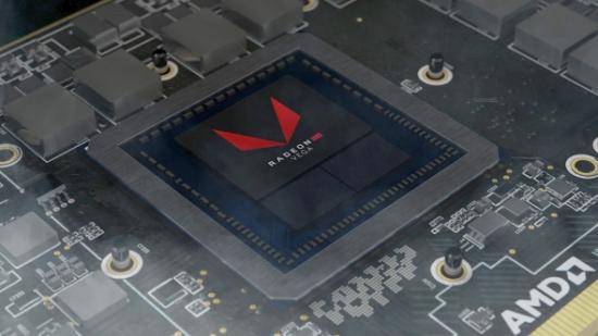
But if the 12nm LPP node can deliver higher density and greater efficiency that would be welcome for both the current-gen Vega and Zen architectures. The Vega GPU could do with running a little cooler and chow down on less power – in a similar way to the rapid refresh of Nvidia’s 400-series Fermi GPUs – and the Ryzen chips would also benefit from a more efficient design, especially if it allows for higher clockspeeds and better overclocking performance too.
Fingers crossed we shouldn’t have to wait long to see the fruits of the AMD/GloFo labours if production really is starting early in the new year.
