It’s only after I’ve handed my passport over to the two gentleman that met me the instant I stepped off the plane, one of whom then wanders off with it into the crowded immigration hall of Israel’s Ben Gurion airport, that I realise I haven’t actually asked who they are. To be fair I have been travelling since 3am, via a very sunny Zurich, and my two-day hangover is very much still in effect.
The codeine pilfered from my parents’ medicine cabinet months ago hasn’t had the calming effect I was hoping for when I first stumbled, skull-throbbing, into the cab to Heathrow this morning, and my guts just feel rotten. The strange mid-flight Swiss Air pastry, dished out alongside something that was almost, but not quite, entirely unlike coffee, hasn’t helped either.
Thankfully the two very helpful, very chatty young men are just fast-tracking me through the packed airport, ensuring their dazed and confused traveller doesn’t find himself lost on the outskirts of Tel Aviv. And they aren’t leading me into a room for an intimate, and unsympathetic, gloved cavity check. That’s always the fear when two random guys pick you up at an airport, right?
But it’s only once I’m standing in front of one of the most light-hearted border control passport prodders I’ve ever met that the scale of what Intel means to Israel starts to become clear. I’ve been tech-ing about the globe for nearly 15 years as a jobbing journalist and I can’t think of another time a border guard has recognised the name of the company I reference while I’m explaining who I’m hoping to meet should they deign to let me enter their country.
“I’m here to visit a company called Intel,” I say.
“Oh, a little company called Intel,” she responds, mocking good-naturedly, “just a small company then. Only little.”
She peers at me through a squeezed-together thumb and forefinger, as if watching the $215bn company squished between her two digits.
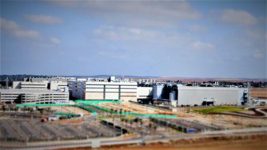
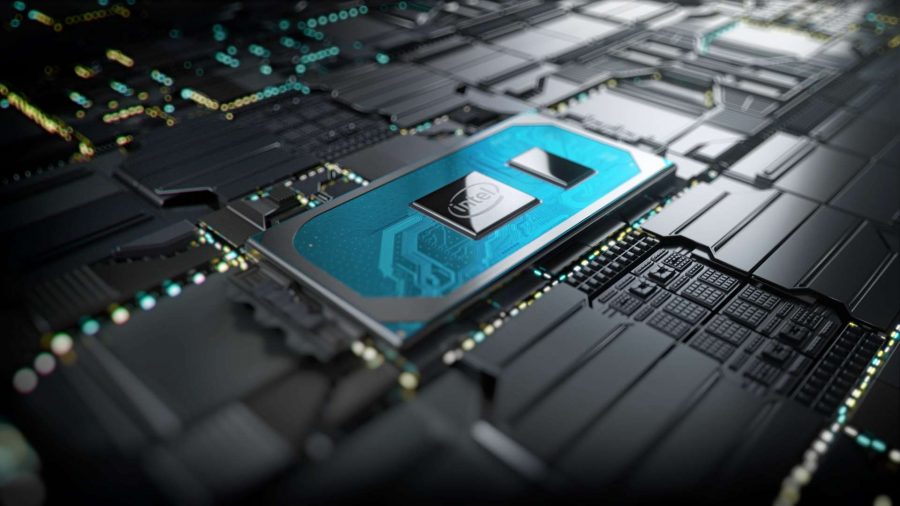
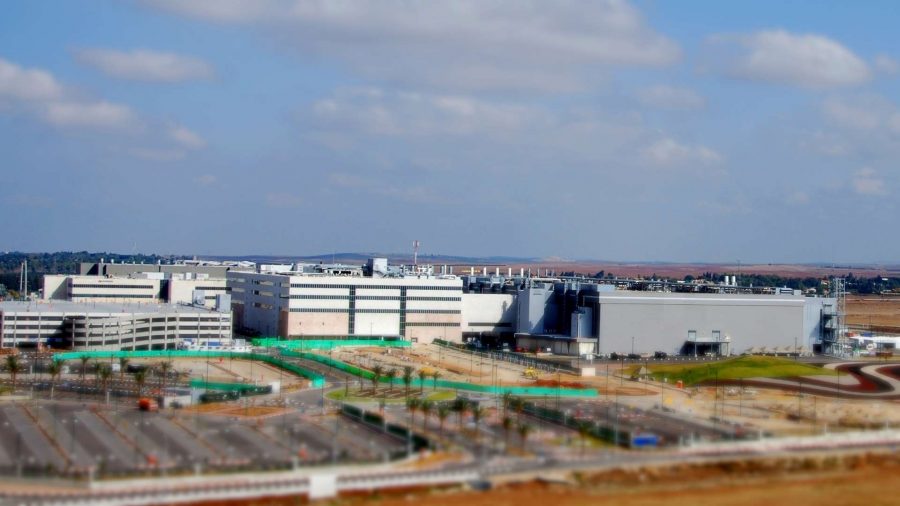
I grin, agree, collect my passport, and I’m out into the blazing Summer heat of Israel and off to the Intel Development Centre in Haifa, then to tread the hallowed halls of Fab 28 in Kiryat Gat, the place where Intel tricks sand into thinking, and where the new 10nm Ice Lake processors are finally flying off the production line.
Intel Development Centre Haifa
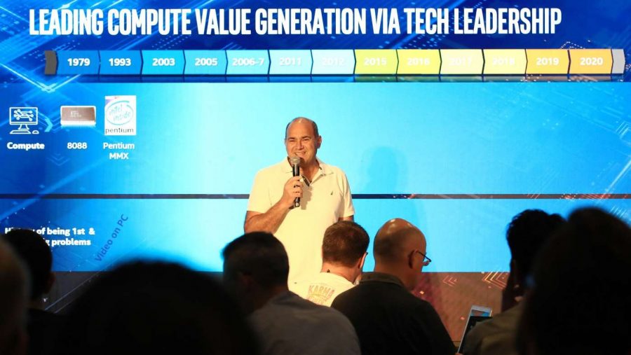
Back in 1974 the Intel Development Centre (IDC) started out as just five employees, now 45 years later it directly employs some 12,800 people and indirectly contributes around 45,000 jobs to Israel’s economy. Of course there are bound to be some financial incentives offered to Intel in order to facilitate its continued presence in the country, but it also brings billions into Israel itself. In fact Intel generates around 1% of the entire country’s GDP on its own.
The first project of any consequence for the IDC team came in 1979 with the 8088. Intel had already released the seminal 8086 chip, but the team in Haifa was tasked with making the 8-bit version of the 16-bit 8086.
“This was the first time that we developed something meaningful for the company,” Intel veteran, Isaac Silas, tells us, “something meaningful that associated with big revenue.”
But the first time that it was really mixing it with the big boys came in 1993 with the Pentium MMX. Prior to this all of Intel’s design and development was carried out in either Oregon or Santa Clara. Before that IDC had to make do with toying around making CPU derivatives for the company.
It was a bit of a rocky start, however. In something that will be familiar to Intel watchers of modern times, the final Pentium product was delayed a year.
“This was not easy by the way,” says Silas. “We didn’t deliver on time. The product was delayed by one year, but it was a big success. And guess what, at that point of time, we didn’t have any competition. So what is one year?”
Then came Centrino. Centrino was a landmark platform for Intel, the first time it wasn’t just creating a single processor – then the Pentium M – but trying to create a platform that has become the template for all modern laptops. It had to be low power, and it had to be wireless.
And it was all developed at IDC in Israel, from the CPU core, to the WiFi part, to the overall integration of the constituent parts. But it was a challenge. The Pentium M was the first design to move from the high-frequency cores of the Pentium 4 desktop chips to low-frequency, but still high-performance cores.
“It was very hard to convince the company how you can have a CPU with a lower frequency, lower power, and beat the high frequency, high TDP CPUs,” recalls Silas. “But this was Banias and we delivered to that.”
And that Banias-codenamed Pentium M core became the basis for the subsequent Core microarchitecture itself which still dominates the CPU market today. Well, we are mighty close to a bit of a CPU revolution right now with AMD’s Ryzen 3000 resurgence, but I think we can all agree the Core design has been pretty successful.
IDC went on to create the first dual-core Intel CPU, and has played key roles in every generation of Core processors ever since, right up to the creation of the 10nm Ice Lake processors which are shipping in laptops this year.
After some very public delays.
The Sunny Cove cores which are at the heart of Ice Lake – and are vital for both the Project Athena devices and the Nervana neural network processor – were developed at IDC. Intel Fellow and director of Core architecture, Adi Yoaz, was laser-focused on pushing single-threaded performance as far as possible with the new CPU design.
“At that time, both in the industry and in academia,” says Yoaz, “there were many doubts as to whether single thread performance can be further improved and whether there are enough sources for IPC, or enough sources for parallelism to continue and push performance on.
“And when we started, we showed that not only can we improve the IPC by big numbers, but also that we have a roadmap of improvements and we can continue to do so for future generations.”
That’s how important Haifa’s IDC is to Intel now, it’s the place where its Core processors have all been born, and where their future has and will be laid out. Intel may get some manufacturing development work done in Oregon, but the bulk of the actual design gruntwork is undertaken in Israel.
Fab 28 Kiryat Gat
Honestly, it’s all been about this moment. The whole reason I’m in Israel isn’t to spend time talking to the super smart engineers responsible for Intel’s finest CPUs. Obviously that’s a privilege and a particular nerdy joy, especially when normally we’re kept away from them by layers of marketing and PR in case we actually experience the dedicated humanity and passion behind the silicon. Heaven forbid.
No, the reason I left my heavily pregnant wife at home with the very real possibility she might burst at any second is because I’ve long craved to see inside one of Intel’s CPU manufacturing plants, and it’s rare indeed that journalists are ever invited in.
And obviously because I’m a very bad person. Sorry, Sarah.
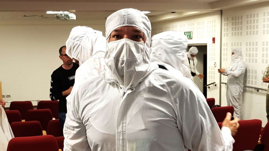
So, there I am inside Fab 28 at Kiryat Gat, standing in an Intel bunny suit, with the hat and the mask over my face reminding me of that time I stood next to Chernobyl’s reactor 4 wishing I had the same all-over protection the power plant staff seemed to be wearing. The suit is too tight and is riding up uncomfortably into my crotch, but I’m still excited. In spite of, not because of. And at least the engineering onesie doesn’t smell too strongly of other people.
But that’s because Intel’s never actually invited journalists into this facility before. No grubby word-wrangler has ever worn this suit before me… and even though it’s a loaner bunnysuit you would expect it to be thoroughly cleaned before it got anywhere near the pristine clean rooms where the multi-billion dollar CPU wafer printing magic happens.
And they probably are. But this one’s never destined to breathe the rarefied air of Fab 28’s clean room. And, sadly, neither am I. The bunnysuit’s just for a quick selfie and a group shot because we can’t be trusted to get anywhere near the actual wafers lest we create yet another long delay for the Ice Lake CPUs which are being printed a few feet away.
That’s kind of a relief to be honest. I get a sort of vertiginous feeling near expensive tech and machinery where I feel like I’m surely going to break something, and maybe not even accidentally.
It’s Daniel Benatar, the general manager of Fab 28, who guides us around the behind-glass window tour of the facility. He’s an engaging and clearly enthused man with sparkling eyes, who’s been with the Israeli branch of the company since the Pentium MMX days of 1993. And he speaks with obvious care, and maybe even slight suspicion, when first introduced to our small band of European hacks.
“One of the new products that we are running here is Ice Lake,” he says. “So we are running it here now in volume manufacturing… It’s the third time. We did 45nm, 22nm, and now 10nm.
“Actually we are doing two technologies in parallel: 10nm and 14nm, the newest technologies in the world. But this is the first time that high volume products transfer from the development side to factories over the sea.”
But he slowly opens up more when he realises we’re just as excited to be there as he seems to be going into work every day.
Around 80% of the tooling has been tuned for Ice Lake now, he tells us. “We are running now thousands of wafers, I cannot tell you exactly the number, but thousands of wafers, every week.”
And how long does it take to turn those wafers into finished Ice Lake silicon?
“It takes a few weeks. I cannot tell you exactly the number because it’s top secret,” he says, a faint smile at the corner of his mouth… like I said, he’s slowly opening up. “But it’s more than two. But we are running it very fast, I can tell you that we are running it very fast. If you compare it to the best in class world performance it’s like one day per mask layer, and we are around that.”
We try asking how many layers there are, but he just laughs, brushing the obvious question aside.
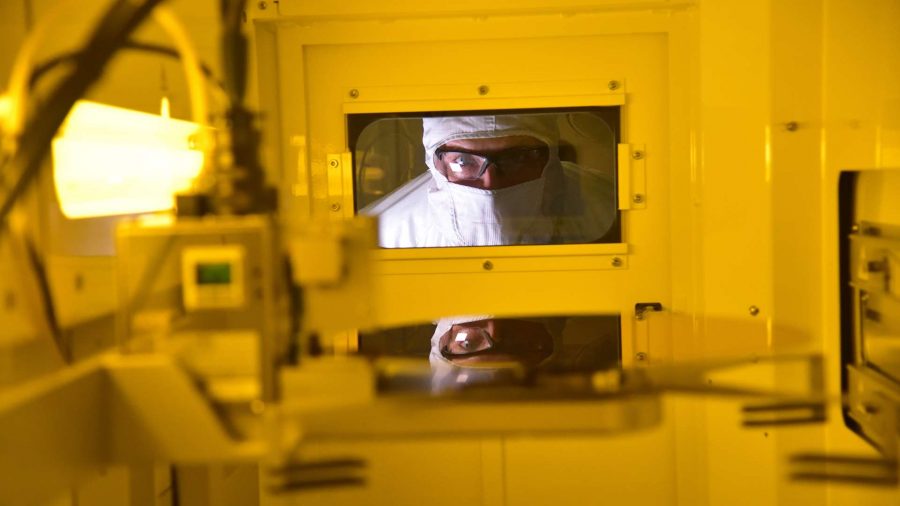
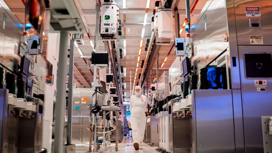
But it’s fascinating seeing the facility as a whole. It’s huge, around 350,000ft2, and we only see a very small part of it on our time nosing about Fab 28. Though, honestly, where the magic happens, where the wafers go through layers of masking, where the actual lithography happens, all that happens inside large ASML-made machines… with animal motifs on the side.
Why the animals? Benatar explains that it’s simply an aide memoir for the engineers working on different floors of the facility. If a machine in the clean room needs to be taken offline for maintenance, or linked machines on the floor below, in the sub-fab, need to be worked on, you need to know which exactly needs the work done. And while it’s possible to remember line codes and numerical references, a frog will likely be more memorable.
That’s important because if you shut off the wrong machine it can literally take days to put them back online and working through wafers.
But we never really get to see those wafers as they go through the extensive, weeks long process of being turned into 10nm processors. The Ice Lake silicon is flying around in little monorail carts set into the roof of the clean room, but packed away from our eyes for its own protection.
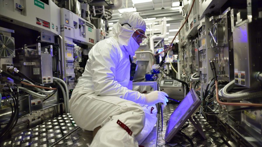
And those guys in the bunnysuits, what are they actually doing in the clean room? Preventing maintenance, essentially. There are a few who are checking wafers straight out of machines, but mostly they are there to ensure things just keep on ticking. The actual functioning of the fab is taken care of remotely, from Remote Operation Centre.
Which is where Benatar takes us next. He’s not meant to. This wasn’t on our scheduled tour and the PR team looks a little flustered as he leads us up to what he calls ‘mission control’ for the entire fab. I’m later told the likelihood of us actually visiting the facility at all was still at about 80% almost as I was boarding my plane at Heathrow the other morning, such was the difficulty getting clearance to show some grubby journos around Intel’s prize chip manufacturing fab, but now we’re being taken to the beating heart of the place.
But it looks like a million other offices. It’s separated out from the other office floors of Fab 28, past the cubicles with the word ‘Yields’ writ large on a sign looming above them. And it’s a secure room filled with computers and multiple screens detailing exactly what’s going on in every machine in the facility.
The place is running 24/7, with workers running in shifts of two days on, two nights on, and four days off. And they’re responsible for the minutiae of ensuring peak production on the station, the lines, that they’re assigned to. Automation is possible, we’re told, but at least for now skilled workers are faster and better able to react to problems or drops in production efficiency than an algorithm is.
As we’re taking all this in Benatar gives the Intel PR team another heart attack. He takes us into a tiny, top-secret room where a crack team of silicon detectives analyse, in microscopic detail, any slight defect in any wafer to track down the source and ensure it isn’t replicated.
Monitors are quickly shut off as it’s perceived we’re maybe taking too keen an interest and with that the tour is at an end. But before we leave Kiryat Gat we get one last unexpected treat: one of Fab 28’s three-times-a-day dance breaks.
As we’re about to leave the Remote Operations Centre, hitherto hidden speakers suddenly start pounding out trance music, and every operator stands up from their station, forgetting the exacting detail of billion dollar production lines still etching wafers somewhere else in this vast building… and they begin to dance.
Join the conversation about Intel’s fascinating 10nm fab by commenting on this article’s Facebook and Twitter threads.
