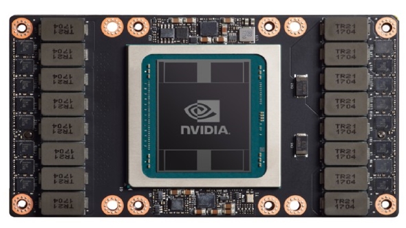
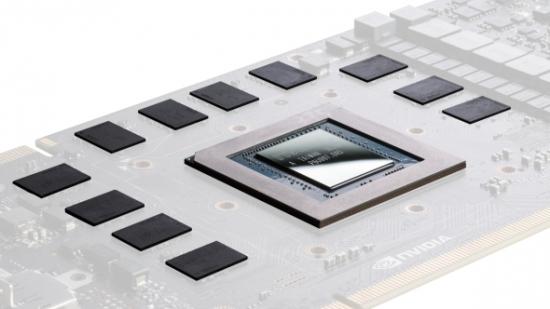
Nvidia likes ‘em big. The first GV100 Nvidia Volta GPU they showed off is a mammoth 815mm², but while the gaming Volta chips aren’t going to be quite that large, they will still be the biggest GPUs you’ll have ever seen on a gaming card.
What’s the best GPU at the moment? Well, this is our pick of the best graphics cards… assuming the crypto-miners haven’t nabbed them all.
When CEO, Jen-Hsun Huang, started waving around the first Volta card, the Tesla V100, at their GPU Technology Conference back in May he was calling it a slice of silicon “at the limits of photolithography, meaning you can’t make a chip any bigger than this.” And, given that even using TSMC’s diminutive 12nm transistor technology the GPU is that damned big, I’m inclined to believe him.
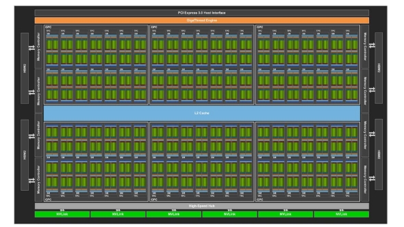
There are, after all, 21 billion transistors inside the V100 chip and a vast number of CUDA cores too. As detailed in the Volta whitepaper Nvidia released this week, the full-fat GV100 GPU sports a total of 5,376 CUDA cores, while the Tesla V100 accelerator is only going to be available using 5,120 of them.
Only 5,120 cores? Pfft, small fry…

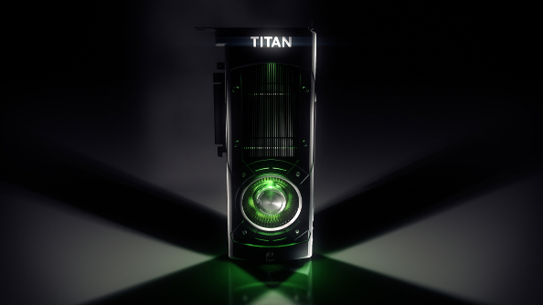
If Volta were to follow the same course travelled by the Pascal party we’d be looking at a Titan Xv being released next year with 5,120 cores. But it’s just not realistic to release a graphics card with a chip the size of the GV100, so the cut-down GV102, which will form the basis of Volta’s Titan cards and a potential GTX 2080 Ti, will have to be much smaller than the 815mm² of the GV100.
With Pascal, the die size dropped from 610mm² to 471mm², going from the GP100 to GP102, and yet still retained the same core count as the professional chip because it ditched both the HBM2 on-die memory and the extra double precision cores.
Even taking that into account (we’re expecting Nvidia to use GDDR6not HBM2 with the gaming cards) the consumer-facing Volta GPUs will need to be around 630mm² if they want to squeeze over 5,000 CUDA cores inside, making them the largest gaming chips Nvidia will have ever produced. And that’s also going to make the Volta Titan a mighty expensive chip to produce, let alone buy.

That ‘biggest chip’ title was previously held by the GTX Titan X and GTX 980 Ti’s Maxwell-powered GM200 GPU. That topped out at 601mm² with 3,072 CUDA cores. On the red side of the graphics divide, AMD’s Fiji GPU was their largest in recent memory at 596mm² with 4,096 of their GCN cores.
There have been rumours that AMD’s competing Vega architecture will release with chips at over 500mm², but they haven’t released any official statements about the real size of the initial Vega 10 GPU.
Of course, the more mainstream consumer Volta variants aren’t going to house a chip of that sort of scale, but they’re still likely to be pretty beefy. If Nvidia follow the Pascal trajectory then the GV104 GPU could still end up being between 420mm² and 480mm².
With the previous generation, the 3,584cores/28 SMs of the GP102 GPU translated into 2,560 cores/20 SMs for the GTX 1080’s GP104, so I’d guess the Volta equivalent would be something like a drop from 5,120 cores/40 SMs to 4,096 cores/32 SMs for a GTX 2080 card.

Though, with Volta, Nvidia have changed from Pascal’s five streaming microprocessor (SM) per general processing cluster (GPC) architecture to one which has seven SM’s per GPC. If they retain this for the more mainstream chips then the GTX 2080 may actually end up at 28 SMs (four Volta GPCs) which would give it the same CUDA core count as the GTX 1080 Ti at 3,584. And that’s got a nice symmetry about it.
But hey, that’s a whole lot of numerical speculation right now, but what we can be sure of is that when Volta does arrive in a more consumer-oriented form it’s going to be huge.
