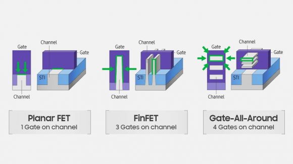
Samsung has succeeded in manufacturing the world’s first 3nm process technology, announcing more details of the advanced process node following a visit by its vice chairman, Lee Jae-yong, to its Research Institute at Samsung’s Mars plant this week. The 3nm design uses a new Gate-All-Around (GAA) technology instead of the classic FinFET transistor design, which is set to offer 30% higher processor performance compared with the upcoming 5nm node.
That 5nm node, set for mass production in the first half of this year, is expected to deliver around 11% higher performance at the same power level as its current 7nm design. That’s a little behind TSMC’s estimates for its own 5nm node, which is touted as offering another 15% higher performance in the same power envelope. This is because Samsung’s 5nm design isn’t a full node successor to 7nm, while TSMC’s 5nm is.
But that seems to be because Samsung is putting all its design weight behind the new 3nm process because that’s where it believes it might be able to make inroads into TSMC’s dominance as the go-to semiconductor foundry for the industry. Samsung’s been very public about its aim of being the number one by the end of this new decade… but it’s got some catching up to do.
The report comes from the Korean press (via HWBattle) with Samsung claiming the 3nm node will deliver a 35% reduction in die size compared with its current 5nm node, while also reducing the power draw by a hefty 50%. Or, if the power is left at the same level, the 3nm node can deliver a 30% increase in processing performance.
We don’t know who’s signed up to use the 3nm GAAFET process yet, but Samsung was trying to woo the great and the good of the tech world its way by giving out the design kit for the 3nm node back in May of 2019. This would allow prospective clients to get a look at what level of design work would be needed, and what benefits they would see, in creating chips using the advanced node.
Samsung’s 3nm process is the first to step away from the traditional FinFET design Intel essentially kicked off with the 3D Tri-Gate transistors in its 22nm Ivy Bridge generation of CPUs back in 2012. The Gate-All-Around design provides a four-sided gate electrode structure that allows more finegrain control over the flow of electricity than FinFET, something that’s vital to the ever-shrinking size of modern transistors.
Whether this will be enough to convince the likes of Nvidia and AMD to shift more of their manufacturing from TSMC to Samsung is unknown right now, but the power outage just a few days before this announcement at its Hwaseong plant probably hasn’t done a lot to instill confidence in its capabilities…
Nvidia is set to use Samsung for some of its next GPUs, but CEO, Jen-Hsun Huang, confirmed in a recent interview that TSMC would still be responsible for the majority of its next-gen 7nm GPU orders.
So yeah, still a long way to go before Samsung can claim that number one spot…


