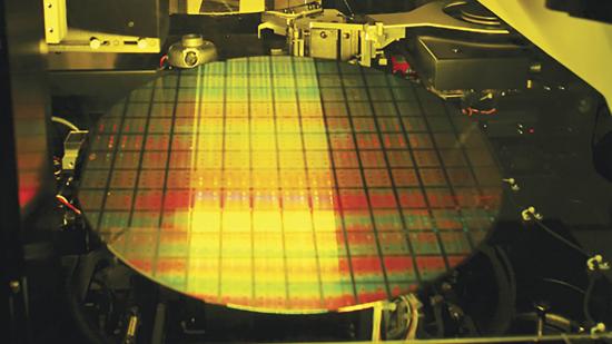
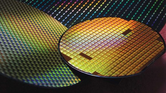
TSMC’s head of marketing believes lithographic process node naming convention needs to change in the near-future. The company’s most advanced node today is 7nm, or N7, which is used across AMD’s Ryzen and Navi range, but soon it will be shifting to 7nm+ (N7+), 5nm (N5), and then onto 3nm (N3). Following that same cadence, where does a foundry go after 1nm, and will it be representative of the physical silicon?
While there are a few nodes left before the naming singularity, even these are controversial. There’s no industry standard naming schema for silicon manufacturing, which allows manufacturers to chop and change process node naming with relative ease to fit marketing purposes.
When asked about the relationship between 7nm and the physical transistor size during an AMD ‘Meet the Experts’ webinar, head of marketing at TSMC, Godfrey Cheng, responded: “ever since 0.35 micron, the number associated with the node has really not been represented by the physical description. 7nm or N7 is an industry standard term for this generation node. The next one will be N5 and then there are a few more nodes beyond that.
“And then I think we need to look at a different descriptor for the nodes beyond what we currently see today.”
Unrepresentative naming is such a widespread and noted issue, Intel published a blog post titled: “let’s clear up the node naming mess” in 2017. Its reasons for doing so were obvious, too. That’s way back when the company was wrestling with its heavily-delayed and ambitious 10nm process node – which is still yet to make its way into the best CPUs for gaming even today. The node is way up there with competitors’ 7nm nodes, if not surpassing them, in terms of actual transistor density.
In said blog post, ex-Intel director of process architecture and integration, Mark Bohr (who retired in 2019), posits that the industry requires a “standardized density metric to level the playing field,” in order to combat companies that have advanced process node names without any increase in density. “Customers should be able to readily compare various process offerings of a chip maker,” Bohr continues, “and those of different chip makers. The challenge is in the increasing complexity of semiconductor processes, and in the variety of designs.”
Intel backs a transistor density naming convention: logic transistor density in units of MTr/mm2 (millions of transistors per square millimetre). This takes into account Scan Flip Flop count/area and NAND2 (two-input NAND) count/area, while SRAM cell size should be reported alongside as a separate metric.
No one else has taken Intel up on its “previously accepted formula for transistor density” so far, yet there’s a turning point swiftly approaching. Perhaps it’s a pipe dream and we’ll just see more of the same marketing spiel when it comes to process node naming in the future, but wouldn’t be nice to actually know what’s going on beneath the surface in an easy-to-parse and comparable format?
Images courtesy of Taiwan Semiconductor Manufacturing Company, Limited.

