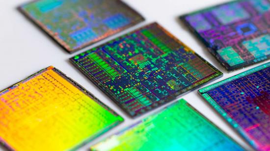
TSMC has taken the wraps off its next process node after the 7nm design being used for AMD’s next-gen Ryzen 3000 processors, and the 7nm+ EUV design set to be used for the Zen 3 CPUs in 2020. Can you guess what it is? Yes, this time we’re talking 6nm EUV.
Now if you’re starting to get a creepy feeling that maybe this is going to be more of a marketing-based name change than a genuine change in transistor size – something akin to the switch between 14nm and 12nm – then I’m right there with you. TSMC has, after all, claimed the new lithography is going to be fully compatible with the design rules of the existing 7nm tech, so products built on the previous lithography can be iterated upon very quickly.
That said, TSMC is promising around 18% higher logic density from the 6nm parts, which could perhaps indicate more of a genuine real world die-shrink. That, and the fact that TSMC isn’t expecting to even get to risk production until the first quarter of next year. Though the density boost does seem in line with what was promised from the EUV-based 7nm+ design, so I’m still a little confused about what the difference actually is between 7nm+ and 6nm. Especially considering TSMC’s 5nm node is already under risk production at the moment and should appear before 6nm… these transistor numbers are starting to lose all meaning to me.
The short announcement piece has appeared on the ever-reliable DigiTimes site, and doesn’t really go into much more detail other than saying that TSMC is targeting both high-performance computing and GPUs with the new production process. Given the timing, and the expectation that Zen 3 is going to be based on 7nm+, AMD’s subsequent GPU and CPU generations could arrive on a bleeding edge node if it were to ship in 2021. Whether that bleeding edge would be at 6nm or 5nm I’m not sure.
Read more: These are the best gaming headsets for your ears
Though that’s probably a little too soon for the expected AMD Navi refresh coming next year, which would leave both Zen 3 and Navi 20 sitting on the same 7nm+ EUV lithography. Which, by all accounts is an impressive node in its own right… though that is also causing me some headaches.
The recent story about TSMC’s 7nm+ design from CommercialTimes suggests that by utilising EUV technology that production process would offer an increase in transistor density of around 20%. That’s around what the 6nm EUV design is set to offer, which makes me question what the benefit of going from 7nm+ to 6nm would be.
It’s possible that the new DigiTimes report is confused, and 6nm will offer 18% greater transistor density over 7nm+ rather than the straight 7nm lithography. That would make it a far more exciting technology bump, but it’s also possible that there is actually very little difference between the 6nm and 7nm+ nodes beyond a pure marketing decision to go up against the new process designs of the competition.
After all, TSMC isn’t alone confusing the living hell out of people with process node advancements. Samsung has just announced that its 5nm EUV design is complete and ready for customer sampling. And that it’s also collaborating with partners on a 6nm EUV node. Meanwhile its 7nm EUV design will be out next year with Nvidia reportedly onboard as a launch partner.
That means next year Samsung will be manufacturing 7nm, 6nm, and 5nm parts, all in various stages of volume and risk production. And from the looks of things they’ll all be IP compatible so partners can design for one and it will be easily migrated across the silicon ecosystem.
Samsung’s 5nm EUV design will reportedly offer a 25% increase in logic density over its 7nm EUV process, but who knows what 6nm will offer… 18% maybe?
Whatever happens, with Nvidia seemingly putting its faith in Samsung’s new processes and AMD siding with TSMC, we could be looking at a 7nm battle royale next year, or even a 6nm one. Or 5nm. I need a lie down.
*header image by Fritzchens Fritz

