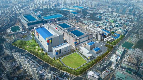
Samsung is reportedly dealing with defects in its foundry products – and that doesn’t look good for its burgeoning foundry business. According to the report by Business Korea, the defects stemmed from the use of contaminated equipment on one of the firm’s 8-inch wafer lines located in the company’s Giheung Plant.
According to a Samsung Electronics official the contaminated process has been cleaned up, preventing any further damage. Contamination of this kind is often disastrous, as the results of foreign particles making their way into the lithographic chip-making process is only spotted in the final wafer, and each contaminated wafer could contain hundreds of dies. Samsung estimates the recent damage to tally at billions of Korean won – or millions of US dollars.
One industry insider speculates that the damage could be far greater than initial reports, however. They claim “Samsung has not calculated the exact amount of the damage yet,” and that “the loss can be much larger than the company’s estimate.” We won’t know the full extent of the damage likely until Samsung’s next financial reports come around.
What’s likely going to miff Samsung Electronics the most is any impact this may have on its reputation. Samsung has pledged itself to becoming the largest semiconductor foundry in the world by 2030. Hitting that milestone would entail kicking AMD and Nvidia foundry partner, TSMC, out of the hot seat. That’s no easy feat, and the company needs to make a name for itself as the best foundry going if it wants to scoop more than its current share of the market.
TSMC ranks third in the list of top semiconductor manufacturers behind Intel and Samsung – both bolstered by first-party manufacturing. In terms of pure-play foundries alone, those that deal in third-party chip manufacturing exclusively, TSMC is top dog.
Even the biggest and baddest aren’t entirely safe from contamination, however. TSMC stumbled earlier this year after operating a portion of its fabs on dodgy photoresist material. This set the company back hundreds of millions of dollars.
One of the major clients shifting to Samsung familiar to us PC gamers is Nvidia. The GPU giant has confirmed it will be utilising Samsung’s 7nm process for its next-gen graphics cards. So far, it seems that 7nm data centre GPUs will be first on the agenda out of Samsung’s fabs. However, rumour has it gaming GPUs, perhaps by the name of Ampere, will follow later in the year.
Any production Samsung may theoretically be operating for Nvidia in the meantime is likely unaffected by the 8-inch wafer contamination. Larger wafers are often utilised for production of cutting-edge nodes and processors associated with modern PC gaming.
