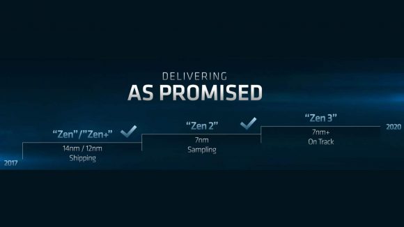
TSMC has already started volume production of its next generation 7nm process; the first to incorporate its advanced EUV tech, and the node which should form the basis for AMD’s Zen 3 processors next year. The Taiwanese contract manufacturer started mass production of the 7nm+ process in March this year, which is a huge milestone for the technology, and it’s being used to create HiSilicon’s phone SoC, the Kirin 985. And if you don’t know who HiSilicon is, you’ll probably recognise its parent company, Huawei. Even if you’re not necessarily sure how to pronounce it correctly.
AMD isn’t kicking off the launch of its upcoming Ryzen 3000 series processors with TSMC’s new 7nm+ EUV process, instead it’s using the more-established 7nm production node this time around. As this is set to be the first volume production run using the 7nm+ process it makes sense to use it on a smaller, lower frequency chip design to start off with.
But what’s the point in this whole Extreme Ultraviolet (EUV) lithography? Well, it’s all about the masks, allowing for fewer manufacturing stages, increased density, and reduced power consumption. All the good stuff, in other words. Oh, and the possibility that it will cater for our silicon needs all the way down to a theoretical 1nm transistor size.
The production run, and density gains, of the 7nm+ design were first mentioned by Commercial Times (via Digitimes) where its report states that mass production began back in March, with 5nm testing production also starting and set to enter volume delivery in some form in 2020. Again, that’s going to be too early for AMD’s next processors, sporting the Zen 3 design, with those chips set to be the first CPUs to deliver on the promise of EUV.
Read more: These are the best CPUs for gaming right now
EUV is all about making it easier to create the sort of miniscule transistors that we need to keep Moore’s Law rolling ever onwards (downwards?), which should also make the resulting products cheaper to produce. Hopefully.
TSMC isn’t going wholeheartedly into this brave EUV future straightaway, however, as the 7nm+ design is only going to utilise EUV for a few layers of masks (the design templates used in CPU manufacturing) and not the whole lot of them. Even so, TSMC claims that its 7nm+ design will still allow for chip creators to increase transistor density by 20% and reduce power consumption by 10% under the same operational load.
Samsung is working hard to ensure that its own EUV efforts make waves, and have reportedly signed Nvidia up as launch partners for 2020, while Intel is also expanding its own 7nm EUV manufacturing, pumping billions of dollars into its own fabs.

We don’t know what level of EUV lithography Samsung and Intel will use for their own 7nm designs, but TSMC’s basic introduction will at least give AMD’s Zen 3 processors the “modest device performance opportunities” its CTO, Mark Papermaster, was touting last year.
Zen 3, the next generation of AMD CPUs, will arrive sometime in 2020, giving the new Ryzen 3000 processors a little time in the sun before they’re replaced by something shinier, denser, and on the whole more extreme.

