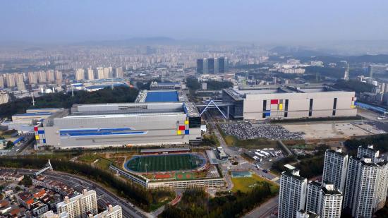
Samsung has nearly doubled how much it’s prepared to spend completing a new production line at its Hwaseong plant, taking the total cost to $1.29bn. Eesh. The line, which is expected to be operational by April 2020, is a part of a colossal six trillion KRW investment in the plant, set for “state-of-the-art infrastructure including Extreme Ultra Violet (EUV) equipment.”
Samsung announced it would be accelerating its plans to upgrade the semiconductor fab back in 2017, and spending the equivalent of over $5bn USD to meet burgeoning demand. The memory market is a little different now, with a global oversupply and slow demand accounting for a fallout in revenue for the global giant. It may even lose its IC throne to usurper Intel, reportedly set to clamber its way back to the top of the market.
But the development at its Hwaseong fab should help the company stay ahead of the game, with the latest EUV production helping it achieve process density of 7nm and smaller in the years to come. And since Samsung offers its fab space out to fabless chip designers, some of your gaming chips may well come from this very fab in the future.
Nvidia is believed to have signed on as a launch partner for Samsung’s EUV process in 2020, while AMD is also now weapons-free to utilise Samsung’s production since amending its Wafer Supply Agreement with GlobalFoundries.
Related: These are the best CPUs for gaming to date
EUV technology has been on the ‘cusp’ of implementation for years, seemingly forever to be touted as ‘just a few years out’. However, 7nm and denser process nodes, 5nm and 3nm, will see the technology actually implemented across many semiconductor manufacturers’ fabs, including Samsung, TSMC, and Intel.
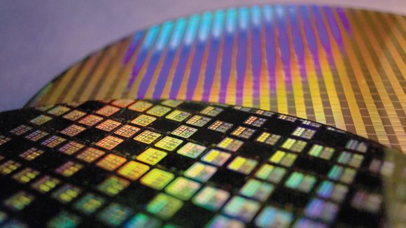
The technology utilises a much, much shorter wavelength (13.5nm) than contemporary lithography by today’s standards (193nm). The gist of the tech is the shorter wavelength allows for fewer stages in the manufacturing process, reducing the need for time-consuming, complex multi-patterning or masking.
AMD is launching AMD Ryzen 3000 CPUs and AMD Navi this year on TSMC’s 7nm process node, while Intel is set to launch another 14nm CPU, Intel Comet Lake, before it moves onto 10nm with Sunny Cove. None of which are utilising EUV during the manufacturing process. Nvidia’s Turing GPUs are also currently built on the non-EUV 12nm process from TSMC.
At least AMD and Nvidia are likely to make the shift to EUV-enhanced technologies with following generations – and there are rumours of both companies considering Samsung for next-gen product.
Intel has said it will make the move over to 7nm EUV on schedule despite its delay in shifting over to 10nm, which is set to launch in volume by the end of 2019. The company has invested big in 7nm EUV, investing billions of dollars into its own fab expansion in Oregon.

