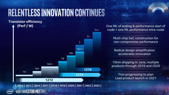
Intel CEO, Bobert Swan, has reiterated the company’s plan to get the “next generation of manufacturing improvements” ready in about two years. That chimes with the 2019 Investors’ Day promises where it claimed the new 7nm process would get its first outing in 2021. Alongside some 10nm++ improvements on the current node.
Swan also cited “a more and more aggressive goal” for the original 10nm process technology as the reason behind the delays of the advanced node. It was hella aggressive, Intel was looking to add in a whole bunch of changes at the same time as shrinking the process node. And, not only that, but it was trying to shrink it down further than traditional scaling would lead you to expect.
Intel called it Hyper Scaling, and this aggressive moves on towards the 10nm lithography was asking its engineers to get 2.7x transistor density improvement over the previous 14nm generation. And that’s why the 10nm node, originally scheduled for launch in 2015, is only now seeing a mobile launch this year.
“At a time when it was getting harder and harder,” says Swan at the Fortune Brainstorm Tech conference, “we set a more and more aggressive goal. From that, it just took us longer.”
The original plan was to get 100 million transistors per mm2 for the 10nm node which would have kept it 3.5 years ahead of the foundry competition and would create a process which would be more advanced that the 7nm designs then coming out of Global Foundries, TSMC, or Samsung.
That temporal lead has evaporated, though Intel will still lay claim to some parity with its 10nm design against the 7nm node that AMD is using for its new Ryzen 3000 processors and the Radeon RX 5700-series graphics cards.
And with Intel itself still promising to move on towards its own 7nm design in 2021, that would potentially put it head-to-head with the 5nm lithography being promised by both Samsung and TSMC.
But Intel sees this fresh competition as a good thing for all concerned. Sure, it’s not happy about the delays to its 10nm node, but the fact the whole industry is pushing forwards can only be a good thing as everyone is trying to find ways to deal with the very real physics barriers that all foundries are fighting against.
“I think that the competition is good now,” says Daniel Benatar GM of Fab 28 in Israel, the place where Intel teaches sand to think in 10nm. “it’s good for all of us. The competition is good because it drives the industry to some nice places.
“The physics that we are dealing with today, you’re trying to print a line of 10nm with 193nm wavelengths. So the physics is the same for all the companies, there’s no secret about what we are doing, or TSMC is doing, or Samsung, or Qualcomm. The physics, it’s very challenged to go to those dimensions unless you will grow. And that’s what the industry is trying to do, to go to EUV. And I believe that we need to go to this.”
Join the conversation and comment on Intel’s process node funtimes on this article’s Facebook and Twitter threads.

